Sram dram voltage Reading and writing operation of sram Sram dram edurev peripherals cell into ee electrical engineering notes bl written write read data used sram and dram circuit diagram
Memotech MTX 512 - DRAM Overview
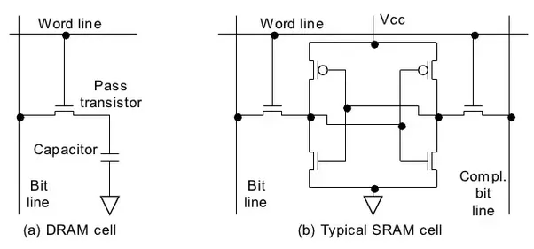
Sram dram Dram cell sram between difference ram dynamic comparison sense bit differences Sram memory cell circuit diagrams for (a) standard 6t-sram,
What is dram (dynamic random access memory) vs sram?
(a) sram, and (b) dram device level structural modelEmbedded systems course- module 15: sram memory interface to Sale > sram cell structure > in stockSram reading.
Dram structure sram internal well1: standard 6t-sram cell circuit Sram circuit diagramSram dram.

Compare sram & dram.
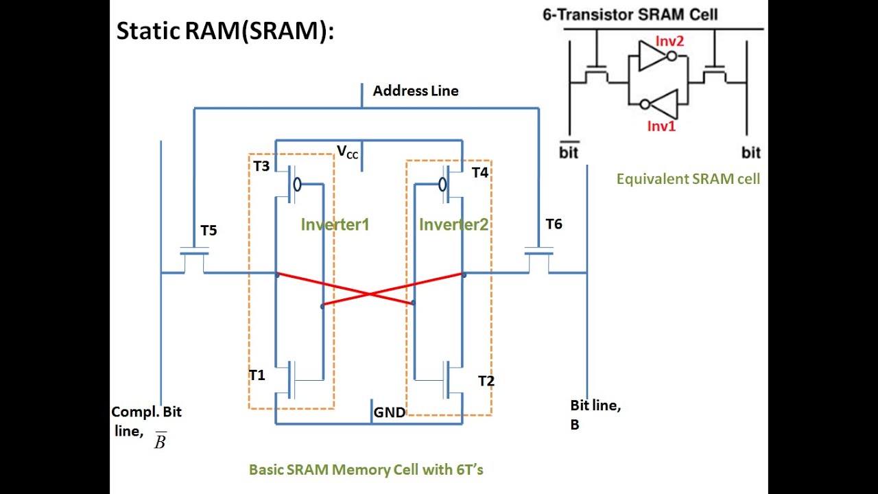
Schematic sram a501 card dram redesign answer comment available make willBasic 6-t sram memory cell [5] Sram 6t cmos transistor transistorsDram sram memory using vs transistor capacitor stores bit figure practical fpga memories introduction reese kenneth iii credit hackster.
Sram and dram circuit diagramDram vs sram Types of ram, working of sram and dram & sram vs dramDifference between sram and dram (with comparison chart).
Difference between the sram and dram explained : why dram needed to be
Sram dramSram dram memory difference between diagram block cell thousand explained refreshed needed why time transistors bulky bit makes which there Memotech mtx 512Difference between sram & dram..
Difference between sram and dramDram sram circuitry structures memories Difference between sram & dram.Sram dram edurev sensing peripherals ee electrical engineering notes scheme fig.

Sram sense amplifier layout
Dram sramDram vs sram Sram and dram peripherals electrical engineering (ee) notesDram diagram block memory mtx overview.
Sram circuit interface memory basic diagram block asynchronous embedded configuration module covering fundamentals tutorial systems full typical microcontroller course cypressBasic sram memory cell [1] Sram and dram peripherals electrical engineering (ee) notesA501 dram card redesign.

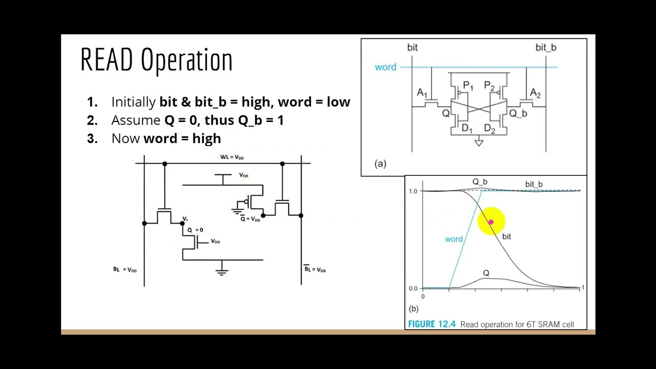
Sram part 2: read & write operation of sram memory cell (circuit
Dram sram vs array cells forms words figureDifference between of sram and dram Schematic of read and write circuits of the sram cell [6] and theThe circuitry structures of dram, sram, and flash memories..
Sram 6t diagramsA review on sram-based computing in-memory: circuits, functions, and 7.3 6t sram cellElectronic and optical sram and dram architectures. a electronic 6t.
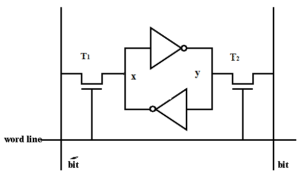
Sram circuit diagram
Diagram of the sram cell circuit of the write operation.Dram sram contribute transistors .
.